在上一个教程中,基本组合算术电路详细讨论了像半加法器,完整的加法器,半减法器和全额减法器一样。现在,在本教程中,将考虑对所有这些电路的布尔表达的真实表和推导。借助派生的布尔表达式,所有这些电路实际上将使用数字IC进行设计。
As discussed in the previous tutorial, the half adder can be constructed using an EX-OR gate and the AND gate. The full adder can be constructed using an OR gate, two EX-OR gates and two AND gates. The half subtractor can be constructed using an EX-OR gate, a NOT gate and an AND gate. The full subtractor can be constructed with an OR gate, two EX-OR gates, two AND gates and two NOT gates. So, for testing all the circuits, two AND gates, two EX-OR gates, two NOT gates and an OR gate are required. For AND gate, 7408 IC can be used which has four AND Gates in-built. For OR gate, 7432 IC can be used which has four OR gates in-built. For EX-OR gate, 7486 IC can be used which has four EX-OR gates in-built. For NOT gate, 7404 IC can be used which has six NOT gates in-built. The input to the digital circuits built from these ICs can be given from a DC supply of 2V while the supply voltage to the ICs can be given from a DC supply of 5V. The 5V DC supply can be constructed using a battery and 7805 IC. The same voltage can be dropped for inputs using a variable resistor. The output can be checked by connecting LEDs at the respective digital output pins.
因此,让我们开始使用上述数字IC测试基本组合电路。
成分Required-

Circuit Diagrams-
这半加法器具有以下电路图 -

Fig. 1: Circuit Diagram of Half Adder
这Full Adder具有以下电路图 -

Fig. 2: Circuit Diagram of Full Adder
这half subtractor具有以下电路图 -

图3:半减法器的电路图
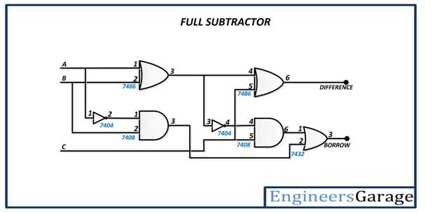
这满减法器具有以下电路图 -

图4:全减法器的电路图
电路连接-
所有组合算术电路都是通过互连逻辑门来构建的。每个组合电路都有自己独特的真实表,其中每个输出都通过某些布尔函数链接到输入。电路是通过互连逻辑门IC构建的。以下逻辑门IC用于电路的构建 -
7408 IC-这7408 IC has quad 2-input AND gates. The IC has the following pin configuration –

图5:7408 IC的表列表销型配置
IC具有以下针图 -
Fig. 6: Pin Diagram of 7408 IC
IC需要5V的电源电压,最多可耐受7V。对于高逻辑的输入和门的输入的电压必须为2V,低逻辑的电压为0V。对于高逻辑,对高逻辑的输出和门的电压为3.4 V,低逻辑的电压为0.2 V。IC在正逻辑系统上运行。从输出处的低水平转移到高水平时的传播延迟为27 ns,而在输出处从高水平转移到低水平的传播延迟为19 ns。
7432 IC- 7432 IC具有四边形2输入或门。IC具有以下引脚配置 -

Fig. 7: Table listing pin configuration of 7432 IC
IC具有以下针图 -
Fig. 7: Pin Diagram of 7432 IC
IC需要5V的电源电压,最多可耐受7V。高逻辑的输入或门的输入的电压必须为2V,低逻辑必须为0V。OR门的输出的电压为3.4 V,对于高逻辑,对于低逻辑,电压为0.35 V。IC在正逻辑系统上运行。从输出处的低水平转移到高水平时,传播延迟为3至15 ns,而传播延迟在输出处从高水平转移到低水平也是3到15 ns。
7486 IC- 7486 IC具有四边形的2输入前门。IC具有以下引脚配置 -

图8:7486 IC的表列表销型配置
IC具有以下针图 -
图9:7486 IC的针图
IC需要5V的电源电压,最多可耐受7V。对于高逻辑,前门输入的电压必须为2V,低逻辑必须为0V。对于高逻辑,前门的输出的电压为3.4 V,对于低逻辑,电压为0.2 V。IC在正逻辑系统上运行。如果其他输入较高,则在输出处从低水平转移到高水平时的传播延迟为23 ns,如果其他输入为高,而传播延迟,而传播延迟,则在输出下从高水平转换为17 ns,则如果其他输入为17 ns,则如果其他输入很高,则为22 ns。
7404 IC- 7404 IC有六个反转门。IC具有以下引脚配置 -

Fig. 10: Table listing pin configuration of 7404 IC
IC具有以下针图 -
图11:7404 IC的针图
IC需要5V的电源电压,最多可耐受7V。这voltage at the inputs of NOT gates must be 2V for high logic and 0.8 V for low logic. The output of the NOT gates have a voltage of 3.4 V for high logic and 0.2 V for low logic. The IC operates on positive logic system. The propagation delay while transiting from LOW to HIGH level at the output is 22 ns while propagation delay while transiting from HIGH to LOW level at the output is 15 ns.
必须注意的是,所选的IC具有兼容的输入,输出和电源电压水平。它们取自数字IC的一个共同家庭(74xx系列)。
这半加法器is constructed by connecting the inputs to an EX-OR gate (pins 1 and 2 of 7486 IC) and an AND gate (pins 1 and 2 of 7408 IC). The Sum bit is drawn from output of the EX-OR gate (pin 3 of 7486 IC) and the carry is drawn from output of the AND gate (pin 3 of 7408 IC).
这full adder is constructed by connecting the inputs to one EX-OR gate (pins 1 and 2 of 7486 IC) and one AND gate (pins 1 and 2 of 7408 IC). The output from first EX-OR gate (pin 3 of 7486 IC) is connected to input of second EX-OR gate (pin 4 of 7486 IC) and input of second AND gate (pin 4 of 7408 IC). The Carry input is connected to another input of the second EX-OR gate (pin 5 of 7486 IC) and other input of second AND gate (pin 5 of 7408 IC). The sum bit is drawn from output of the second EX-OR gate (pin 6 of 7486 IC). The output from second AND gate (pin 6 of 7408 IC) is connected to one input of OR gate (pin 1 of 7432 IC) and output from first AND gate (pin 3 of 7408 IC) is connected to other input of OR gate (pin 2 of 7432 IC). The carry out is drawn from output of the OR gate (pin 3 of 7432 IC).
半减法器是通过将输入连接到EX-OR门(PINS 1和7486 IC中的第1和2)的构建的,并将一个输入连接到不栅极的输入(7404 IC的引脚1),然后将一个直接连接到AND AND GATE的输入(7408 IC的引脚2)。来自GATE的输出(7404 IC的引脚2)连接到和门的输入(Pin 1 of Pin of 7408 IC)。差位是从Ex-Or Gate(7486 IC的引脚3)的输出中得出的,借款是从和门的输出中得出的(7408 IC的引脚3)。
完整的减法器是通过将输入连接到第一个ex-Or Gate(PINS 1和7486 IC中的第1和2)的构建,并将一个输入连接到第一个不栅极的输入(7404 IC的引脚1),然后将一个输入直接连接到第一个和第一和第一的输入门(7408 IC的引脚2)。First Not Gate(7404 IC的引脚2)的输出连接到第一和门的输入(7408 IC的引脚1)。从第一个前门(7486 IC的引脚3)发出的输出连接到第二个前门的输入(7486 IC的引脚4)和第二个不栅极的输入(7404 IC的引脚3)。携带输入连接到第二个前门(7486 IC的引脚5)和第二和门(7408 IC的引脚5)的另一个输入。差位是从第二个前门的输出中得出的(7486 IC的引脚6)。从第二和栅极(7408 IC的引脚6)输出连接到一个或门的一个输入(7432 IC的引脚1),并连接到第一和门的输出(7408 IC的引脚3)已连接到或GATE的其他输入(引脚2 of 7432 IC)。借用是从OR Gate的输出中得出的(7432 IC的引脚3)。
电路如何工作-
每个组合电路都有自己的真相表和对输出的各自布尔表达式。上面构建的电路及其预期输出将在下面讨论 -
半加法器
这binary adder is the basic arithmetic circuit as the operation of adding binary numbers is a fundamental task in computing. The binary addition follows the following rules –
0 + 0 = 0
1 + 0 = 1
0 + 1 = 1
1 + 1 = 10
在前三个操作中,每个二进制添加都给出一个位,即0或1。但是第四个添加操作给出了一个由两个二进制数字组成的总和。在这种情况下,较低的显着位称为总和位,而较高的显着位称为携带位。
这半加法器有以下真相表 -

图12:一半加法器的真相表
From the above truth table, the following K-map are drawn for deriving the boolean expressions for the sum and carry output –
图13:k-map的总和为一半

Fig. 14: K-Map for Carry Out in Half-Adder
因此,总和和携带输出的布尔表达如下 -
SUM = A’B + AB’ or SUM = A b
b
携带= ab
所以,二进制加法器构造g在这个项目ives a sum with carry. This Half adder has two inputs for the two bits to be added and two outputs one from the sum ‘ S’ and other from the carry ‘ c’ into the higher adder position. In the circuit for half adder, the carry signal from the addition of the less significant bits is drawn from the output of AND gate while the sum is drawn from the output of the EX-OR Gate.
Full Adder
完整的加法器是形成算术输入之和的组合电路。它由三个输入和两个输出组成。一个完整的加法器一次一次添加三个位很有用,但是半加法器不能这样做。完整的加法器具有以下真相表 -

图15:完整加法器的真相表
From the above truth table, the following K-map are drawn for deriving the boolean expressions for the sum and carry output –
Fig. 16: K-Map for Sum in Full-Adder

图17:K-Map for Carry Out in Full-Adder
因此,总和和携带输出的布尔表达如下 -
SUM = A’B’C + A’BC’ + ABC
= a’(B’C
bC’) + A(BC’
公元前)
= a’(B
C)+ A (b
C)
= a
b
C
CARRY = A’BC + ABC + ABC’ + AB’C
= AB + A’BC + AB’C
= ab + c(a
b)
= AB + BC + AC
半减法器
这half subtractor is constructed using X-OR and the AND Gates. The half subtractor has two input and two outputs. The outputs are difference and borrow. The difference can be applied using X-OR Gate, borrow output can be implemented using an AND Gate and an inverter. The half Subtractor has the following truth table –

图18:半减法者的真相表
从上面的真实表中,绘制了以下k映射,以得出差异和借用输出的布尔表达式 -
图19:K-Map for Difference in Half-Subtractor

图20:k-Map借入半提取器
因此,差异和借用产出的布尔表达如下 -
差异= a’b + ab’
借用= a’b
完整的减法器
这满减法器is a combination of X-OR, AND, OR, NOT Gates. In a full减法器逻辑电路应具有三个输入和两个输出。将两个半减法器放在一起提供了完整的减法器。完整的减法器具有以下真相表 -

Fig. 21: Truth Table of Full Subtractor
从上面的真实表中,绘制了以下k映射,以得出差异和借用输出的布尔表达式 -

Fig. 22:k映射全额提取器的差异

Fig. 23:k-Map借入全额提取器
因此,差异和借用产出的布尔表达如下 -
差异= a
b
C
借用= A’B + BC + A’C
Testing the circuits-
可以通过通过7805电压调节器为ICS给ICS的电源电压来测试上述组合电路。相同的电压可以使用高逻辑的可变电阻降至2V级,同时通过地面提供低逻辑。可以通过在每个组合电路的输出引脚处连接LED来检查输出信号。可以通过验证每个电路的真相表来检查电路。
在下一个教程中,了解代码转换器电路。
Circuit Diagrams

提交以下:精选贡献